| |
|
|
|
|
|
|
Digital hardware systems can be viewed from many alternative perspectives, including Boolean logic, logic gates, and behavioral specifications. We will use Alliance, a set of tools for VLSI design in which logic functions are constructed from CMOS technology, the dominant technology of today for high-density logic circuits, primarily because the transistors can be very small, allowing for VLSI designs.CMOS technology provides two types of transistors: n-channel transistors that use negatively-charged electrons for current, and p-channel transistors that conduct current by means of positively-charged holes. CMOS structures have become the primary switching devices in high-density IC design because:
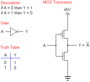
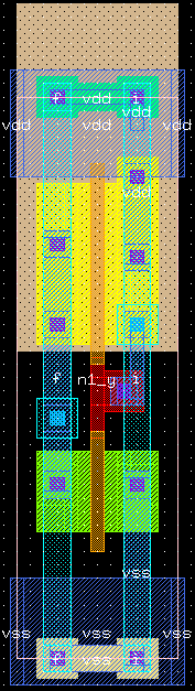
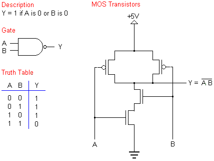
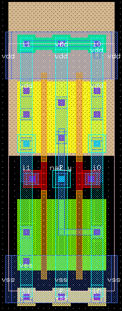
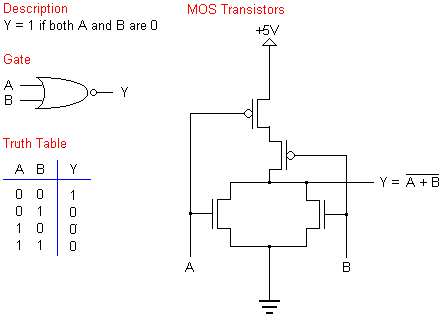
Any logic gate can be constructed from a combination of nMOS and pMOS transistors in a common substrate. Figure 1 shows the functional description, the gate representation, the truth table, the transistor network and, the standard cells in Alliance for (a) an inverter, (b) a two-input NAND gate, and (c) a two-input NOR gate.
These networks establish the foundation for building larger circuits since all Boolean functions can be implemented in terms of AND, OR, and NOT.
Chip ArchitectureVLSI design is based on hierarchy and incremental approaches: To deal with complexity and different power requirements, every chip is composed of two major blocks: the first is called the core, which embodies the chip's functionality; the second one is called the pads, which provide the means to exchange signals with the core. In turn, the core could be further partitioned into two sub-blocks, according to its specific design requirements: the control unit and the data path.Figure 2 shows the partitioning approach to the design when using Alliance:
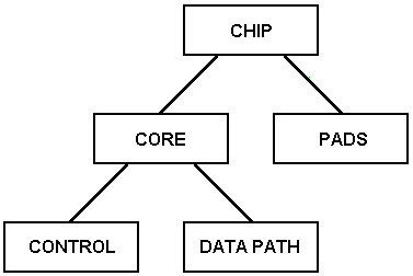
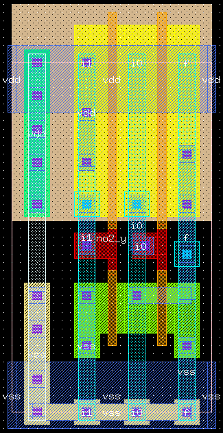
Figure 2. Alliance's first partitioning approach Usually at the core level, the leaf cells of the design belong to the Alliance standard cells library and describe the logical functions needed to design the circuit.. At the chip level, the previous core and pads belonging to the Alliance pad library are used. The circuit netlist will be captured in two steps:
Alliance does not uses a schematic editor for netlist capture, but rather a textual approach. To do so, Alliance handles among others the following file formats:
Design Examples
|
|||||||||||||||||||||||||||||||||||||||||||||||||||||||||||
|