Home Page
Control Circuit and Protocol for Structural Testing
of Integrated Circuits Using Terminal Characteristics
Adrian Virgil CRACIUN
Transilvania University of Brasov, Electronics and Computer Department
Selections (
The Circuit |
Specifications )
Abstract: This paper presents an original circuit used to control a structural integrated circuit's test The test method is based on plotting the integrated circuit (IC) current-voltage terminal characteristics. The control circuit includes an original dynamic logical level shift circuit that can be used to transfer data from a bus into a latch. Based on the control circuit timings analyze, an original protocol, used by the test control software, was developed. All analyzes were made on the real implemented circuits.
Key Words: Logical level shift circuits, IC testing.
The structural IC test system
Structural testing is based on modelling faults and simulating the fault effect on the overall behaviour in the test conditions. Structural testing reduces the test sequence by collecting the smallest set that covers the most modelled faults.
The proposed test method verifies the behaviour of the tested IC at its terminals. ...
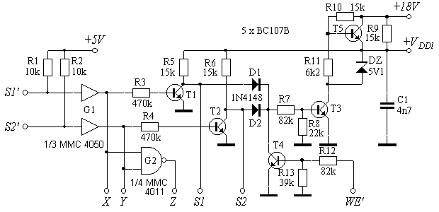
Figure 2 presents the control circuit schematics.
Three lines of the control SPP bus are connected at the circuit input and 6 control signals are generated at its output. The input signals are: S1', S2', WE'; The ' index (negate) means that "0" is the active state.
Three of the output signals are used to control the digital multiplexer: X', Y' and Z' are the selection signals for D-MUX. The other three: S1, S2 and VDDl signals decide where and when the current code and the current address (from the same Data bus) are latched. VDDl signal is used as a power supply for the CMOS latches. This signal and the latches STROBE signals (S1 and S2) realize a dynamic logical level conversion circuit which convert the TTL signals from SPP to high voltages CMOS signals. This circuit is used instead of 8 statically conversion circuits (for the 8 lines of Data bus).

Fig. 2. The schematics of the control circuit
The dynamically logical level shift circuit is based on applying a variable power supply to CMOS latches. When the data arrive from the SPP (TTL level) the latch is powered with 5V voltage, STROBE input is active (S1' or S2' is "0") and the input data are memorized. The next step is to deactivate the STOBE input and to rise the supply voltage to the desired value (near 18V in this case).
The latches used in this circuit must have internal transfer gates that disconnect the data inputs from the rest of the IC when STROBE input is not active (for example MMC 4042 or MMC 4508). If latches without internal connection gates at their inputs are used, the IC-s supply current raises when a 5V voltage is applied at the input of an 18V-power supply IC. This 5V is "0" logic (less than 1/3 of 18V) but is also in the input voltage domain where both NMOS and PMOS transistors (of the internal inverting gates) are opened and the IC supply current can rise up to 15 mA for a buffered latch IC.
The input signals are applied through 2 non-inverting buffer gates (1/3 of MMC 4050) which convert the TTL signals in CMOS (0-5V) signals with R1 and R2 [2]. The CMOS buffers output signals are X', Y' and Z' (Z' = X + Y, realized with G2 NAND gate).
The dynamically logical level shift circuit is realized with T1, T2 transistors that acts as inverters powered at a variable supply voltage and with D1, D2 and T3 that acts as a NAND gate
The T5, R10 and R11 circuit reduces the transient T3 switching time and provides a supplementary current (than the one through R9) when VDDl is lower than a certain value. This circuit allows the increasing of R9, reducing the supply current for the whole circuit without affecting the transient performances. The divider resistors R10 – R11 must realize the cutoff of T5 when T3 is saturated.
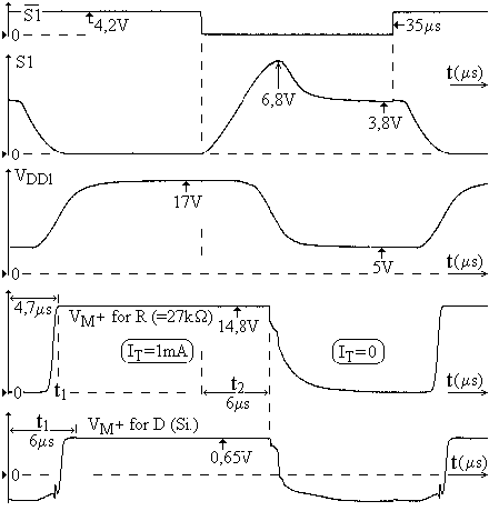
The transient performances can be analyzed from figure 3, where some signals acquired from a digitally oscilloscope (acquired with a GPIB connection) are presented.

Fig. 3. Experimentally signals of control circuit
S1' signal is switched between the two states with a 14 kHz frequency and S2' = 1 (not active). The test voltage VT is represented when a resistor, respectively a diode is connected between the test points. From the test circuit point of view it is important only the period when the current generator is active (in this case after IT = 1mA current appears). According with the figure 3, a 5…6 microsecond delay appears from the moment the command is initiated until the test voltage get stable.
The C1 capacitor reduces the supply line noise but also produces the transient regime degradation and a few nF value for C1 is a good compromise.
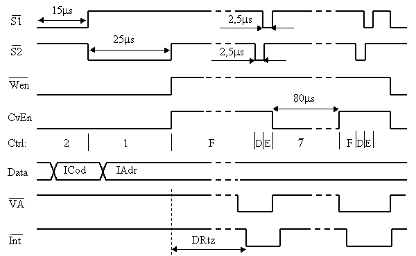
The command sequences for writing the data in the latches and for reading the test results, presented in figure 6, are denominated as a "measurement" (for a specific test combination ICod and IAdr). ( top )
Greater delays than the minimum necessary ones (presented in the previous paragraph) are used:
- For a strobe signal shift a 15ms was chosen (instead of 5…7 m s as the ones in figure 3),
- For simultaneous strobe signals shift a 25
ms was set (instead of 11ms delay from figure 4).

Figure 6 The control signals timing for a typically measurement,
without supplementary readings
A safety coefficient of two was used, for a safe command without getting exaggerated supplementary delays.
A "measurement" algorithm includes the next steps:
- The interface programming, consists on ICod and IAdr latching;
- Waiting the interrupt request (Int.) signal,
- The first result reading (Res_0), a reading sequence (3 steps and data processing);
- A new acquisition start after approx. 80ms delay, using "CvEn" control signal;
- The next result reading (Res_1), necessary to verify if the transient regime ends;
- The actual result is compared with the previous one, two cases can be found:
- Different results, the algorithm will be continue at step 4,
- Identically results (2 LSB accepted error), the next step will be executed;
- The result is processed and memorized;
- End of procedure, return to the main program.
A special situation the program must deal with is when no "Int." request appears. In that special situation (that can appear when an oscillation is produced between the tested pins, and the VA circuit don't start the acquisition) an error code is memorized after a time-out (about 0.1s) and the procedure ends.
The subroutine was written in assembling language. This subroutine can measure the transient regime length (TRLng, with 0.02…1.2ms experimentally values, depending on the tested IC and pins). The software delays were calibrated with a special procedure in the initialization phase.
The "Ctrl" line in figure 6 present the hexadecimal values of control word (modified with XOR function with the mask "0B"hex in order to consider the inverted bits at the SPP Control bus).
Conclusions
A specific protocol was developed for structural IC testing using I-V terminal characteristics and an original circuit for dynamically logical level shift of bus data to be latched was realized and practically verified.
Home Page
